Skip to content
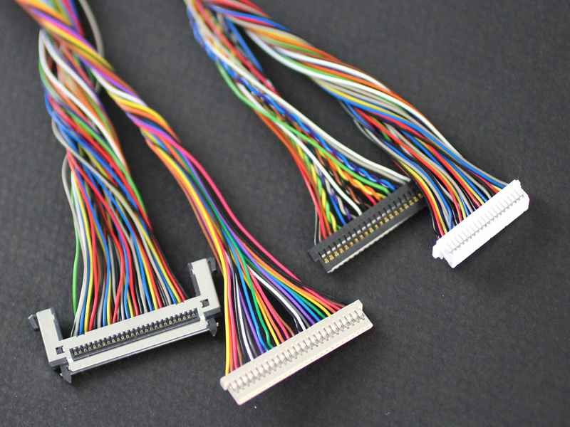
LVDS is widely chosen because differential signaling is good at rejecting noise, yet that reputation can hide an important practical detail: an LVDS link is only as balanced as the physical channel carrying it. Between the transmitter and receiver are PCB breakouts, fine-pitch connectors, stripped termination zones, cable pairs, shields, grounds, bends, clamps, and nearby power circuits. A small asymmetry in any of these areas can turn a clean differential link into a source of common-mode current, electromagnetic radiation, or reduced signal margin. That is why a cable can pass continuity testing and still fail an EMC test, or work on a bench and become unstable after installation inside the final product.
LVDS cable common-mode noise is usually caused or amplified by imbalance in the differential path, including pair skew, unequal impedance, connector discontinuities, asymmetric coupling, poor shield or ground transitions, and mechanical changes to cable geometry. The most reliable way to reduce it is to preserve pair symmetry, control differential impedance, provide an intentional return path, minimize mode conversion, and validate the complete link with signal-integrity and EMC measurements appropriate to the application.
A useful way to think about the problem is to imagine two nearly identical runners carrying the same message in opposite directions. As long as they stay together, outside disturbances affect them almost equally and the receiver can ignore much of the interference. The trouble starts when one runner takes a longer path, passes through a different doorway, or gets pushed closer to a noisy machine. In real LVDS systems, those small physical differences are skew, discontinuity, grounding, and routing. The sections below show how to find those differences before they become a production problem.

What Is Common-Mode Noise in an LVDS Cable?
Common-mode noise in an LVDS cable is the unwanted voltage or current that appears in the same direction on both conductors of a differential pair. A balanced LVDS receiver rejects much of this shared disturbance, but problems arise when the common-mode level exceeds device limits, common-mode current radiates as EMI, or cable and connector imbalance converts part of the shared noise into differential noise that the receiver cannot reject.
| Parameter | Typical LVDS Reference | Practical Meaning |
| Differential impedance | About 100 ohms | Common target for many LVDS links; verify the actual interface specification. |
| Driver current | About 3.5 mA | Representative classic LVDS current-source value. |
| Differential swing | About 350 mV | Representative classic LVDS signal amplitude. |
| Nominal common-mode level | About 1.2 V | Typical operating center for classic LVDS implementations. |
| VDIFF | VP – VN | Voltage difference interpreted as the data signal. |
| VCM | (VP + VN) / 2 | Average voltage shared by the two conductors. |
| Receiver common-mode range | Device-specific | Always verify the exact receiver datasheet. |
Common-Mode vs Differential Voltage
LVDS is easier to understand when the two conductors are separated into differential and common-mode components. If the instantaneous voltages are VP and VN, differential voltage is VDIFF = VP – VN, while common-mode voltage is VCM = (VP + VN) / 2. Suppose VP is 1.375 V and VN is 1.025 V. The pair carries 350 mV differential voltage around a 1.20 V common-mode level. If 150 mV of interference couples equally onto both wires, both voltages rise, but their 350 mV difference remains essentially unchanged, so an ideal receiver still sees the same logic information.
The difficulty appears when the disturbance is not equal. If 150 mV couples onto one conductor but only 100 mV reaches the other, 50 mV of differential disturbance has been created. That number can matter far more to the receiver than the original common-mode shift. Classic LVDS implementations commonly use a differential termination near 100 ohms, a driver current around 3.5 mA, and a differential swing around 350 mV, but these are representative values rather than universal limits. Actual common-mode input range, threshold, and operating margin must be checked against the specific transmitter and receiver datasheets used in the system.
How LVDS Rejects Shared Noise
LVDS gains much of its noise immunity from physical symmetry. The positive and negative conductors are kept close together and carry complementary currents, so an external electric or magnetic field tends to couple a similar disturbance into both. The receiver subtracts one input from the other, removing much of the shared component. The same symmetry also helps reduce radiation from the link because equal currents flowing in opposite directions create fields that partly cancel in the surrounding space. This is the basic reason a well-built differential pair can operate reliably in an electrically noisy product without needing a large signal amplitude.
The cancellation is only as good as the balance of the real channel. If one conductor is longer, closer to ground, more heavily loaded by a connector contact, or separated farther from its partner near a termination, the two paths stop behaving the same way. A surprisingly short transition can therefore undo some of the benefit provided by a long section of well-controlled cable. In practice, the final few millimeters of untwist, the contact geometry inside a fine-pitch connector, the board breakout, and the shield termination can matter as much as the nominal cable impedance printed on a datasheet.
When Common-Mode Noise Matters
Common-mode voltage is not automatically a failure. If it remains within the receiver’s allowed common-mode range and stays nearly equal on both conductors, the receiver may continue to decode the signal correctly. Problems usually appear through one of three mechanisms. The input can move outside the receiver’s permitted range, common-mode current can use the cable and surrounding chassis as a radiating structure, or asymmetry can convert the shared disturbance into differential noise. The last mechanism is especially important because once noise becomes differential, it directly reduces the voltage and timing margin used for data detection.
This is why a single oscilloscope reading labeled ‘common-mode noise’ rarely tells the whole story. Engineers need to know the common-mode level, the differential eye or waveform that remains at the receiver, and the balance of the path that connects the two ends. Mechanical conditions also belong in that picture. Tight bends, compression under clamps, shield openings, connector strain, and uneven termination can all change how the two conductors interact with their surroundings. A robust LVDS cable specification therefore controls pair identity, polarity, impedance, critical geometry, shielding, and connector orientation rather than relying on continuity and nominal cable type alone.

What Causes Common-Mode Noise in LVDS Cables?
Common-mode noise in LVDS cables usually comes from electrical or mechanical imbalance somewhere in the differential channel. Pair skew, unequal loss, impedance discontinuities, excessive untwist, asymmetric connector transitions, poor shielding, unstable ground references, cable deformation, and nearby switching sources can all create common-mode energy or convert differential energy into common mode. The root cause is therefore often channel imbalance rather than the LVDS transmitter itself.
| Root Cause | Electrical Effect | Typical Observation | Useful First Check |
| Intra-pair skew | Timing imbalance and mode conversion | Eye closure or higher EMI | Delay or eye comparison |
| Connector discontinuity | Reflection and asymmetric loading | Ringing or local impedance step | TDR |
| Excessive untwist | Pair balance and impedance change | Higher susceptibility near termination | Visual and dimensional inspection |
| Unequal loss | Amplitude imbalance | Reduced eye height | Waveform or S-parameter comparison |
| Poor shield bond | Larger common-mode return loop | Radiated-emission peak | Shield and shell continuity |
| Nearby switching source | Asymmetric field coupling | Failure only in certain operating states | Source ON/OFF test |
| Cable deformation | Geometry and impedance shift | Bend-sensitive failure | TDR before and after movement |
Pair Skew and Timing Imbalance
Intra-pair skew occurs when the two conductors in one differential pair do not have the same electrical delay. The cause may be physical length mismatch, unequal dielectric conditions, inconsistent twisting, different connector paths, or an asymmetric board breakout. Skew becomes more serious as the timing window becomes smaller. At 500 Mbps, one unit interval is 2 ns, so 100 ps of skew consumes 5% of one UI. At 1 Gbps the same 100 ps consumes 10%, and at 2 Gbps it consumes 20%. These percentages are examples, not acceptance limits, but they show why the same physical mismatch becomes more significant as signaling speed rises.
Skew also creates a temporary current imbalance during transitions. In an ideal pair, one side rises while the other falls at nearly the same time, preserving the equal-and-opposite relationship that keeps the link quiet. If one edge arrives earlier, there is a brief interval when the pair no longer cancels cleanly, so additional common-mode content can appear. This is why length matching should be treated as part of the electrical timing budget, not merely as a mechanical drawing tolerance. For multi-channel LVDS harnesses, pair-to-pair consistency matters too, especially when clock and data relationships are sensitive to accumulated delay.
Impedance and Connector Discontinuities
A cable built from nominally 100 ohm differential material does not automatically remain 100 ohms through the finished assembly. The geometry changes where the pair enters a connector, where insulation is stripped, where wires are spread toward terminals, where solder or crimp geometry changes, where a shield is opened, and where an overmold or clamp compresses the cable. Every abrupt change can reflect part of the travelling waveform. If both conductors see exactly the same transition, the effect may remain mostly differential, but real contact geometry and nearby ground structures are rarely perfectly symmetrical, so part of the disturbance can appear as common-mode energy.
Connector transitions deserve special attention because they are often the least controlled part of an otherwise controlled cable. A fine-pitch connector may require the pair to spread apart, change reference geometry, or pass through contacts with different parasitic capacitance and inductance. Excessive untwist increases the same risk by changing both conductor spacing and local coupling. The practical design goal is not to create a mathematically perfect transition, which is rarely possible, but to keep the transition short, symmetrical, repeatable, and compatible with the system margin. TDR comparison between an approved sample and a failed sample can be especially useful when a problem repeatedly appears near a connector.
External Coupling, Ground, and Mechanics
External interference usually couples most harmlessly when the pair is physically balanced. A twisted pair routed away from high-current switching conductors may receive almost the same disturbance on both wires. If one conductor is moved closer to a motor lead, DC/DC switching node, backlight inverter, or VFD cable, the coupled voltages become unequal and the difference appears as differential noise. This explains many bench-versus-installation problems: the cable works while lying in free space, then becomes unstable after the final product forces it into a tight route beside a stronger electromagnetic source.
Ground and shield design can create another path for common-mode current. An interrupted shield, a long inductive pigtail, poor connector-shell bonding, or a ground strategy that does not match the chassis architecture can force current through a larger unintended loop. Mechanical deformation can add still more asymmetry by altering pair spacing or dielectric geometry under a clamp, sharp bend, or overmold. In real troubleshooting, the useful question is not simply ‘Is the cable shielded?’ but ‘How is the pair balanced, where does common-mode current return, and which physical feature changes when the failure appears?’

How Does Common-Mode Noise Affect EMI and Signal Quality?
Common-mode noise affects LVDS in two main ways: it can drive common-mode current that radiates from the cable and causes EMC problems, and it can be converted into differential noise by an unbalanced channel. The second effect reduces eye opening, increases jitter, and lowers receiver margin. A link can therefore appear functionally normal while still radiating too much energy or operating with very little remaining margin.
Common-Mode Current and EMI
A balanced differential pair is naturally favorable for EMC because the intended currents are nearly equal and opposite. With the conductors close together, their fields partially cancel. Common-mode current behaves differently because both conductors move in the same effective direction relative to the surrounding structure, so the return path may flow through a shield, chassis, ground wire, cable tray, or parasitic capacitance. That return path can be physically much larger than the spacing within the differential pair. As a result, even a comparatively small common-mode current can become a more efficient radiator than the much larger intended differential current.
This is the reason a product can show a perfect image and still fail radiated-emissions testing. The receiver may be rejecting the shared voltage correctly while common-mode current is using the cable as part of an antenna structure. Shield coverage alone does not guarantee success because the termination determines whether the shield actually provides a low-impedance path at the troublesome frequency. A braided or foil shield that ends in a long pigtail can perform very differently from the same material bonded through a short circumferential connection. EMC debugging therefore needs to follow current paths, not only signal voltages.
Signal Margin and Mode Conversion
The receiver usually fails when the differential margin becomes too small, not simply because common-mode voltage exists. Cable attenuation reduces amplitude, reflections distort edges, skew narrows timing margin, asymmetric coupling introduces differential noise, and ground offset shifts the input toward the edge of its permitted operating range. Each effect may be modest by itself, yet their combination can close the eye. This is especially important with LVDS because the signal swing is intentionally small. Representative classic LVDS differential amplitude is around 350 mV, so tens of millivolts of differential disturbance can represent a meaningful fraction of the available signal.
Margin also changes with cable length, connector choice, temperature, component variation, and installation. A prototype that works on a short cable in a quiet lab may have little reserve after the production version becomes longer or the final enclosure places it closer to a switching source. Good engineering therefore asks how much margin remains rather than whether the link merely works today. When common-mode noise is suspected, the most useful measurements pair a common-mode or current observation with a differential metric such as eye opening, jitter, BER, or system error rate.
Display Symptoms and False Clues
Display artifacts are visible, but they are not unique fingerprints of common-mode noise. Flicker, intermittent horizontal or vertical lines, corrupted frames, unstable startup, or image loss can also come from incorrect pair mapping, reversed polarity, connector contact problems, excessive attenuation, clock-data timing error, panel power disturbance, or ground-reference problems. The operating condition usually provides the stronger clue. If the image fails every time a motor starts, electromagnetic coupling becomes more likely. If touching the connector changes the symptom, the contact interface or mechanical transition deserves attention. If a short cable works and the production-length cable fails, loss, skew, and impedance margin move higher on the list.
Functional testing also has a blind spot: a cable can pass a brief system test and still have very little design margin. Continuity testing proves the conductors are connected, but it does not prove differential impedance, skew, shield effectiveness, or high-frequency loss. TDR, eye analysis, BER or long-duration system tests, and EMC measurements each answer different questions. The depth of testing should match the application risk. A short internal display cable in a quiet consumer product may need less characterization than an industrial vision harness routed beside servo drives, but both benefit from understanding which electrical feature is actually protecting the link.
Which Cable Design Choices Reduce Common-Mode Noise?
The most effective LVDS cable choices preserve symmetry across the whole channel. Controlled pair geometry, suitable differential impedance, consistent delay, careful connector transitions, appropriate shielding, a deliberate ground or return strategy, and sensible routing usually reduce common-mode problems more reliably than adding a filter after the design is complete. Cable construction should be selected for the actual interface, length, packaging, environment, and validation target.
Twisted Pair or Micro-Coax
Twisted pair and micro-coax can both support LVDS successfully, but they solve different packaging and electromagnetic problems. A controlled twisted pair naturally helps equalize external coupling because the two conductors repeatedly exchange their physical position relative to nearby fields. When twist, conductor spacing, and dielectric geometry are stable, the pair can maintain predictable differential impedance and good balance. Micro-coax becomes attractive when channel density, connector pitch, cable thickness, or individual shielding dominates the design. High-density display and camera assemblies often use multiple micro-coax elements because they can pass many signals through a narrow mechanical envelope without creating a large round bundle.
The better choice depends on the actual channel rather than a simple rule such as ‘coax is always better shielded’ or ‘twisted pair is always better balanced.’ Engineers should compare target data rate, channel count, connector system, available cross-section, bend radius, required flexibility, shield strategy, termination method, and cost. SINO-CONN’s LVDS development work includes both micro-coax and approximately 100 ohm-class differential twisted-pair structures, with final construction tied to the customer’s interface, pin map, routing space, shielding plan, and validation requirements rather than treated as one fixed catalog cable.
Pair Geometry and Length Matching
Stable pair geometry keeps the two conductors in a similar electromagnetic environment and helps maintain differential impedance. Important variables include conductor diameter, center-to-center spacing, dielectric thickness, twist pitch, shield spacing, and the geometry maintained in the connector transition. Length matching should be considered in terms of delay, not simply millimeters, because propagation velocity depends on the dielectric. The manufacturing target should therefore come from the timing budget. Tightening a tolerance beyond what the system needs can raise cost without improving performance, while leaving a critical delay uncontrolled can consume a large fraction of the available eye opening.
Pair identity is equally important in multi-channel harnesses. Accidentally combining one wire from one pair with a wire from another can still produce correct pin-to-pin continuity while destroying the intended differential geometry. The same risk exists when pair members are separated too early during assembly and routed independently through a connector. Good documentation makes the pair relationship visible in the drawing and work instruction, then controls the dimensions that affect it. Once a prototype demonstrates acceptable eye, impedance, or system performance, those physical features should become part of the released production definition instead of remaining informal knowledge held by one technician.
Shielding, Grounding, and Filtering
A shield is most effective when its current path is understood. Foil provides high coverage with relatively low thickness, braid provides lower resistance and better mechanical robustness, and foil-plus-braid constructions can provide broader performance at the cost of greater diameter, stiffness, and assembly complexity. The connection at the cable ends can matter as much as the material itself. At higher frequencies, a long narrow pigtail adds inductance and may prevent the shield from behaving as the low-impedance bond that the design assumed. Short, wide, or 360-degree connections can be more effective when the connector and chassis architecture support them.
Ground strategy and cable routing should be reviewed at the same time. There is no universal rule that every shield must be grounded identically at both ends; the correct approach depends on chassis architecture, ground-potential difference, safety requirements, and the frequency range of concern. Common-mode chokes and ferrites can help after the main current path is understood, but each component has frequency-dependent impedance, parasitic capacitance, and insertion loss. A useful filter is one that improves the relevant common-mode or EMC measurement without materially reducing differential eye margin. If a choke lowers one emission peak but noticeably worsens jitter or signal amplitude, the design still needs work.
How Do You Measure and Diagnose Common-Mode Noise?
Diagnosing LVDS common-mode noise requires several complementary measurements. Oscilloscope math separates differential and common-mode voltage, TDR locates impedance discontinuities, eye diagrams and BER testing show remaining signal margin, and VNA or EMC tools reveal frequency-dependent loss and radiation. Controlled A/B tests are equally important because they show whether the problem follows the cable, the routing, the grounding condition, or a specific interference source.
| Test Method | Main Question | Strongest Use |
| Oscilloscope VP/VN | What voltage exists on each line? | Common-mode and differential waveform inspection |
| Eye diagram | How much voltage and timing margin remains? | Jitter, ISI, and cumulative signal quality |
| BER or functional test | Does the real link transfer data reliably? | System-level performance confirmation |
| TDR | Where does impedance change? | Connector, bend, untwist, and termination localization |
| VNA / S-parameters | How does the channel behave versus frequency? | Insertion loss, return loss, and channel comparison |
| Spectrum / near-field probe | Where and at what frequency is EMI strongest? | EMC source and coupling investigation |
| Shield continuity | Is the intended shield path complete? | Shell, drain, and bond verification |
Measure the Pair Correctly
Begin by observing both conductors of the same LVDS pair at the same time. From those waveforms, calculate VDIFF = VP – VN and VCM = (VP + VN) / 2. The formulas are simple, but the measurement is easy to corrupt because LVDS amplitudes are small and edge rates can be fast. Probe capacitance, long ground leads, mismatched channels, or an unsuitable reference point can create apparent ringing and noise. Differential probes with adequate bandwidth and low loading are usually the cleanest option, although two matched single-ended channels can also be useful when the setup is carefully controlled.
Location matters just as much as probe quality. Measuring only at the transmitter shows what the source creates, not what the receiver sees after the signal has passed through the connector and cable. Measuring at the receiver is often the best first step because that is where the data decision occurs. If the waveform is poor there, compare it with a point farther upstream. A clean transmitter and distorted receiver suggest the problem developed in the interconnect, while a distorted transmitter points toward the source or PCB. Development hardware that provides deliberate test access can save many hours later during EMC or intermittent-display debugging.
TDR, Eye, and BER
TDR is particularly useful when the question is ‘Where does the electrical structure change?’ A fast edge is launched into the channel and the reflection is translated into impedance versus time or distance. A feature near the connector may indicate a transition problem; a longer shifted region may point toward cable geometry; a new disturbance after bending can reveal mechanical sensitivity. The best use of TDR is comparison. An approved sample, a failed sample, and a revised sample can be overlaid to show whether a manufacturing or design change altered the same physical region where the failure is suspected.
Eye diagrams and BER testing answer a different question: how much usable communication margin remains. Eye height shows voltage opening, while eye width shows timing opening after attenuation, reflection, skew, jitter, and intersymbol interference have accumulated. BER or a long-duration functional test then checks whether the system actually transfers data reliably under realistic conditions. A visually clean eye does not replace functional validation, and a short functional pass does not prove robust margin. For display applications, it can be valuable to pair instrument measurements with real panel operation under the same cable length, routing, temperature, and noise conditions expected in the product.
VNA and Controlled A/B Testing
A vector network analyzer becomes useful when the project needs frequency-domain information about the complete interconnect. With suitable fixtures, measurements can characterize insertion loss, return loss, and more advanced differential or mode-conversion behavior across frequency. This can help distinguish a connector transition problem from bulk cable loss, compare two cable constructions, or evaluate how bending changes high-frequency performance. VNA testing is not mandatory for every short LVDS cable, but it becomes valuable when the interface is faster, the cable is longer, the margin is small, or repeated failures point toward frequency-dependent behavior that a simple continuity or DC resistance test cannot reveal.
Controlled A/B testing is often the fastest route to the root cause because it changes one variable at a time. Compare a known-good cable with the suspected cable, a short cable with the production length, interference source OFF versus ON, original routing versus a physically separated route, and the cable in a relaxed state versus its installed bend or clamp condition. If the failure follows one cable across different systems, cable construction moves higher on the list. If several cables fail only when a motor operates, the electromagnetic environment deserves more attention. Good troubleshooting converts ‘it flickers sometimes’ into a repeatable condition that measurements can explain.
How Do You Fix and Prevent LVDS Common-Mode Noise?
The strongest fixes remove the imbalance that creates or converts common-mode energy. Correct pair skew, control impedance, shorten excessive untwist, improve connector transitions, define shield and ground paths, and change routing where needed. Ferrites or common-mode chokes should be validated only after the dominant mechanism is understood. The final fix should then be frozen into drawings, BOMs, work instructions, tests, and an approved production reference.
Correct Pair and Connector Imbalance
Start with the part of the channel that is measurably different between a good condition and a bad one. If the raw cable already shows excessive skew, the cable construction or supplier specification may need to change. If the bulk cable is stable but the problem appears after termination, focus on strip length, untwist, conductor separation, contact routing, and connector geometry. Useful corrective actions include keeping the pair together for as long as possible, making the positive and negative paths geometrically similar, removing unnecessary stubs, controlling the stripped region, and preventing local compression. The goal is to fix the mechanism, not simply tighten every tolerance on the drawing.
Once a revised sample performs better, convert the successful geometry into something production can repeat. Pair mapping, polarity, critical exposed length, connector orientation, shield treatment, and any timing-sensitive length control should be visible in the controlled engineering definition. SINO-CONN’s LVDS manufacturing framework follows this approach by moving from interface and pinout review through channel definition, cable and connector confirmation, drawing, prototype, electrical or signal validation, and finally production. That sequence helps prevent a common failure mode in custom cable projects: a prototype works because an experienced technician built it carefully, but the production documentation never captured what made it work.
Improve Shield and Ground Paths
If common-mode current is causing EMI, determine where that current is returning before increasing shield complexity. Inspect the entire path from the cable shield through braid, foil, drain, connector shell, backshell, and chassis connection. Look for long pigtails, broken shell continuity, shield removed too far from the connector, inconsistent bonds between prototype and production, or a ground arrangement that differs from the system architecture assumed during design. At higher frequencies, connection inductance becomes increasingly important, so a physically short and broad bond can outperform a longer connection even when both appear electrically continuous on a basic ohmmeter test.
Routing should be included in the same corrective action because moving the cable away from a motor lead, DC/DC switching node, or high-current harness can sometimes produce a larger improvement than changing the shield construction. When separation is limited, reducing long parallel runs and crossing aggressor conductors at a larger angle may reduce coupling. After the modification, repeat the original EMC or functional condition rather than judging success from appearance. A shield or route change is valuable only if it reduces the measured problem while preserving the intended mechanical installation and the differential signal margin at the receiver.
Validate and Freeze the Fix
A laboratory modification is not a production solution until it survives the same condition that caused the original failure and can be manufactured repeatedly. If the problem occurred only with the longest cable, test the longest intended configuration. If it appeared only when a motor ran, validate with the motor operating. If bending triggered the issue, repeat the bend or routing condition. The validation package may include controlled connector part numbers, pair mapping, cable construction, impedance requirement, critical strip or untwist dimensions, shield and ground termination, bend limits, continuity testing, shield continuity, and project-specific TDR, eye, BER, or system-display verification.
Production control closes the loop. A Golden Sample or approved reference is useful when it is tied to a drawing revision, BOM, test method, and measurable critical characteristics rather than treated as a visual sample alone. High-speed cable quality should also avoid silent substitutions: changing connector contacts, raw cable, shield construction, or termination method can alter performance even when the pinout remains unchanged. For teams developing or correcting an LVDS assembly, sharing the connector P/N, pin map, target length, data or clock requirements, grounding strategy, failure condition, and available TDR, eye, or EMC data usually makes the engineering review faster and more focused.
Conclusion
LVDS common-mode noise is rarely solved by looking for one magical component. The most durable solutions come from preserving the balance that differential signaling depends on: matched pair behavior, controlled impedance, short and repeatable connector transitions, intentional shield and ground paths, sensible routing, and validation under the conditions that matter in the finished product. A cable that merely passes continuity or displays an image for a few minutes may still have little electrical margin, while a properly engineered assembly has the critical physical features and acceptance methods defined before volume production begins.
For an existing LVDS problem, the most productive starting package is usually the real system information rather than a request for ‘more shielding.’ Connector part numbers, pin mapping, target cable length, interface or clock rate, board-side mating details, grounding strategy, installation photos, the condition that triggers the failure, and any available eye, TDR, spectrum, or EMC results give an engineering team something concrete to compare. SINO-CONN can use those inputs to review whether the next step should be a pair-geometry change, connector-transition revision, different cable construction, shielding or grounding improvement, targeted filtering, or a controlled validation sample.
Frequently Asked Questions
What is the difference between LVDS common-mode noise and differential noise?
Common-mode noise shifts both LVDS conductors in the same direction relative to the receiver reference, while differential noise changes the voltage difference between the two conductors. A balanced LVDS receiver rejects much of the common-mode component, but it cannot reject noise once imbalance converts it into differential mode. In practice, engineers should examine both VCM and VDIFF, because a modest common-mode disturbance can still become harmful when connector geometry, pair skew, grounding, or external coupling affects the two conductors differently.
Can a 100 ohm LVDS cable still have a common-mode noise problem?
Yes. A nominal 100 ohm differential cable can still develop common-mode problems because the finished channel includes connector contacts, stripped regions, board transitions, shield terminations, bends, and mechanical routing. The bulk cable may be close to its impedance target while a short asymmetric transition creates reflections or mode conversion. For this reason, critical projects may need TDR, eye, or system-level validation of the assembled link rather than relying only on the raw cable datasheet or a continuity test.
Does shielding always reduce LVDS common-mode noise?
No. Shielding can reduce coupling and provide a controlled return path, but its effectiveness depends strongly on termination and system grounding. A shield with poor connector-shell continuity or a long pigtail may provide much less high-frequency benefit than expected. In some systems, grounding choices can also introduce unwanted current paths. The best approach is to review shield construction, end termination, chassis bonding, pair balance, and cable routing together, then verify the result under the actual EMC or operating condition that caused the problem.
Should I add a common-mode choke to an LVDS cable?
A common-mode choke can be useful when measurements show significant common-mode current in a frequency range where the selected device provides useful impedance without excessive differential loss. It should not be the first response to unknown noise. Pair imbalance, connector discontinuities, shield termination, ground return, and routing should be checked first. After adding a choke, compare both the EMC result and the differential signal quality, because a part that reduces one emission peak but closes the eye is not a complete solution.
How can I tell whether an LVDS problem comes from the cable or the system?
Use controlled substitution. Compare a known-good cable with the suspected one in the same system, then compare short and production-length cables, original and separated routing, interference source OFF and ON, and relaxed versus installed cable conditions. If the failure consistently follows one cable, the assembly becomes a stronger suspect. If different cables fail only when a motor or converter operates, the electromagnetic environment, grounding, or system architecture deserves more attention. Repeatable A/B conditions are more useful than random cable swapping.
Which tests are most useful for LVDS cable common-mode noise?
The most useful test depends on the question. Oscilloscope measurements can calculate VCM and VDIFF; TDR can locate impedance discontinuities; eye diagrams show accumulated voltage and timing margin; BER or long-duration functional tests verify real data performance; VNA measurements characterize frequency-dependent loss and reflections; and spectrum or near-field measurements help locate EMI energy. For many projects, the fastest diagnosis combines one signal-integrity test with a controlled A/B system test rather than relying on a single instrument result.
Can cable bending increase LVDS common-mode noise?
Yes, especially when bending changes pair spacing, compresses dielectric material, disturbs a shield, or forces the two conductors into different electromagnetic environments. A normal bend within the cable’s intended mechanical range may have little effect, but sharp folds, tight clamps, over-tight cable ties, or poorly supported connector exits can change local impedance and balance. If a failure is movement-sensitive, compare TDR, eye, or functional behavior before and after the same bend condition and define a practical bend or routing limit for production.