Skip to content
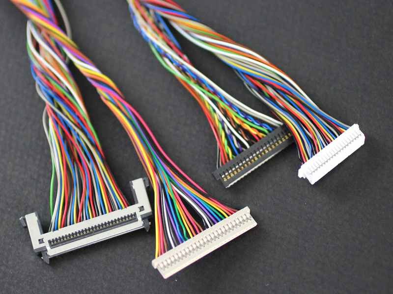
An LVDS display cable can look completely correct and still produce the wrong image. The connectors may mate cleanly, every conductor may pass continuity, and the panel may even light up, yet colors can be wrong, alternating columns can appear out of order, or the display can flicker only after the cable is installed inside the enclosure. That happens because an LVDS display connection is not simply a bundle of wires. It is a coordinated path for pixel data, serialized lanes, differential pair polarity, clock timing, connector pins, grounding, and sometimes two separate links carrying different pixel positions.
LVDS display channel mapping is the process of matching serialized pixel data, differential lanes, clock signals, pair polarity, and, in dual-link systems, odd and even pixel streams between a video source and a display panel. Correct operation requires both the logical data format, such as VESA or JEIDA, and the physical controller-to-panel pinout to agree through the complete cable assembly.
This distinction becomes important during real development work. A team replacing an LCD may discover that the old and new panels use connectors with the same pin count, but the data mapping is different. Another team may build a cable that passes every continuity check but still fails because Link A and Link B were interpreted differently by the source and panel. The fastest route to a stable display is to separate these layers, verify them one by one, and freeze the working definition before the project moves into repeat production.

What Is LVDS Display Channel Mapping?
LVDS display channel mapping defines how pixel information, control bits, differential lanes, clock pairs, connector pins, and dual-link pixel streams are matched between a display controller and an LCD panel. It includes both logical data mapping and physical wiring. A cable may be electrically continuous yet still be functionally wrong when lane identity, polarity, data format, or link order does not match the panel definition.
What Does “Channel” Mean in LVDS?
The word “channel” is used at several levels in LVDS documentation, which is why engineers can talk past one another even when they are looking at the same interface. One datasheet may call DATA0 a channel, another may use “Channel A” for an entire group of data pairs and a clock, and a dual-link panel may describe two complete links as Channel A and Channel B. Before anyone changes a pin table, it helps to establish exactly which layer the word refers to in the project.
A practical hierarchy is straightforward. A conductor is one copper path. A differential pair is two conductors carrying complementary signals. A data lane is one differential pair carrying a serialized LVDS stream. A clock lane is a differential pair carrying the pixel timing reference. An LVDS link combines several data lanes with a clock, while a dual-link interface uses two such links to share the display stream. In many classic display implementations, RGB666 uses three data pairs plus one clock pair, while RGB888 uses four data pairs plus one clock pair, although the actual panel and transmitter documentation always takes priority.
Is Channel Mapping the Same as Pinout?
Channel mapping and pinout are related, but they answer different questions. Channel mapping describes what a signal path carries, while pinout describes the physical connector location where that path appears. A controller might output TX2+ and TX2- on pins 15 and 16, while a panel expects the corresponding RX2+ and RX2- on pins 7 and 8. The cable is correct when the functions match, even though the pin numbers at the two ends are different.
This difference becomes critical when two connector families use different numbering conventions, when one drawing is shown from the mating face and another from the wire side, or when a right-angle cable exit visually mirrors the pin order. A production-ready definition should therefore record connector part number, connector view, pin number, signal name, pair identity, polarity, wire or micro-coax identification, From-To relationship, and ground or shield treatment. Treating color alone as the identifying feature is risky because colors can change during material substitution while the electrical net must not.
Which Signals Are Being Mapped?
RGB information is only part of the story. The serialized LVDS data lanes can carry color bits together with display-control information, while a separate differential clock pair provides the timing reference needed by the receiver. A hybrid display harness may also carry panel power, return paths, backlight power, enable signals, dimming controls, or vendor-specific functions through the same connector. Keeping these groups visibly separated in the drawing makes both engineering review and production testing easier.
For a 24-bit RGB888 display, the color information alone contains 24 bits per pixel: 8 red, 8 green, and 8 blue. In a common single-link display arrangement, four data pairs carry the serialized data and one additional pair carries the clock. RGB666 carries 18 color bits and commonly uses three data pairs plus one clock. These figures describe widespread architectures rather than universal pinouts, so a panel datasheet must still be checked before any cable is released.
| Common Display Format | Color Bits | Typical Data Pairs | Clock Pairs | Typical Total LVDS Pairs |
| RGB666 / 18-bit | 18 | 3 | 1 | 4 |
| RGB888 / 24-bit | 24 | 4 | 1 | 5 |
| Dual-link RGB888 | 24 per pixel stream | 8 total | 2 | 10 |
The cable-level review should also track differential pair assignment, pair polarity, pair-to-pair consistency, impedance target, length matching where required, shield or drain termination, connector direction, and installed routing. Those details are not secondary packaging choices. They determine whether the serialized stream reaches the panel in the same form that left the source, especially when fine-pitch connectors, micro-coax bundles, or tight folding paths are involved.
Which LVDS Mapping Format Is Used?
The correct LVDS mapping format is the one expected by both the transmitter and the panel receiver. VESA or SPWG-style and JEIDA mappings can carry the same nominal color depth while placing RGB bits differently inside the serialized lanes. If the source and panel disagree, synchronization may remain stable even though colors, gray levels, or gradients are visibly wrong, making the issue easy to misdiagnose as a cable defect.
What Is VESA Mapping?
VESA-style mapping is one common method of arranging pixel and control information across LVDS data lanes. In an RGB888 system, 24 color bits must be represented for each pixel, and those bits are serialized across several differential lanes according to a defined bit-position diagram. The receiver reverses that process and reconstructs the red, green, and blue values. If the transmitter and receiver use different diagrams, the physical signal can be present while the reconstructed color values are wrong.
This is one reason panel replacement should never be approved only because both displays are described as “24-bit LVDS” or use the same connector pitch. Two panels can share the same nominal color depth, lane count, and connector size but assign RGB significance bits differently. Vendor terminology can also vary. Documents may use VESA, SPWG, OpenLDI, Format A, Format B, or internal naming. The safe approach is to compare the actual lane and bit mapping illustrations rather than assuming that similar labels mean identical behavior.
What Is JEIDA Mapping?
JEIDA mapping is another established way of arranging RGB and control information in an LVDS display stream. The electrical signaling is still differential LVDS, but the position of significant and less-significant color bits across the lanes can differ from a VESA-style arrangement. This difference becomes especially noticeable when working across 18-bit and 24-bit panel families, because RGB666 contains 6 bits per color channel while RGB888 contains 8 bits per color channel.
A JEIDA or VESA mismatch does not always produce a black screen. The display may remain synchronized, text may stay sharp, and image geometry may look normal while color ramps, skin tones, dark shades, or subtle gradients look noticeably wrong. That is why controlled test patterns are useful during bring-up. Full red, green, blue, white, black, and smooth grayscale ramps expose bit-significance errors far more clearly than a busy photograph, where a technician may simply conclude that the panel has poor color calibration.

How Do VESA and JEIDA Differ?
The main difference is logical bit placement rather than the basic electrical concept of LVDS. Both formats use differential lanes to serialize image data, but they can assign RGB bits to different serialized positions. As a result, statements such as “both are LVDS,” “both are 24-bit,” or “both use four data pairs” are not enough to prove compatibility. The interface has to agree at the level where the receiver reconstructs the pixel values.
A disciplined review normally checks color depth, mapping format, number of data lanes, lane order, pair polarity, clock definition, single-link or dual-link mode, and dual-link pixel order where applicable. If the source device or bridge supports programmable mapping, software may solve the mismatch without changing the cable. If the source format is fixed, the solution may require a different panel, bridge configuration, PCB routing, or interconnect definition. Changing the cable before identifying the incorrect layer can create an unnecessary custom part that later becomes difficult to support.
Which Mapping Does the Panel Require?
The panel datasheet is the primary reference. Useful sections are often named LVDS Input, Data Mapping, Interface Signal, Input Timing, Receiver Data Format, Pixel Data Assignment, or LVDS Bit Mapping. The diagram should then be compared with the source-side definition from the processor, FPGA, serializer, timing controller, or RGB-to-LVDS bridge. If the source is configurable, the active register, firmware, or device-tree setting belongs in the same project record as the cable drawing.
A simple interface record can prevent later confusion by stating the color depth, mapping family, lane count, link mode, dual-link order, source configuration revision, and panel revision in one place. This becomes especially valuable when a display platform remains in production for several years and the original engineer is no longer involved. A future panel substitution can then be evaluated against a known interface baseline instead of relying on a working cable sample whose crossed pins or unusual routing may no longer be understood.
How Are LVDS Lanes Mapped?
LVDS lanes are mapped by tracing every source signal through its connector pin, differential pair, cable path, destination pin, and receiving function. The mapping must preserve pair identity, polarity, clock assignment, expected lane order, and the intended transmission structure. Matching connector numbers alone is insufficient because different ends may use different pin numbering, connector views, or deliberate signal crossovers. internally.
How Are DATA Lanes Assigned?
A common RGB888 single-link display may use labels such as DATA0+/-, DATA1+/-, DATA2+/-, DATA3+/-, and CLK+/-. The transmitter might call them TXOUT0 through TXOUT3, while the panel labels the corresponding receivers RXIN0 through RXIN3. These naming differences are manageable once every function is translated into a controlled From-To table. What matters is not whether both sides use the same label, but whether the correct serialized stream reaches the receiver lane that expects it.
Each differential pair should remain a pair throughout the assembly. DATA1+ should not be bundled with DATA2- simply because the connector positions are nearby or the termination sequence is easier. Pair geometry is particularly important near fine-pitch connectors, where conductors or micro-coax elements must be separated for termination. Excessive untwist, long stripped sections, asymmetric preparation, or a poor transition into the connector can disturb the differential structure even when the pin map itself is correct.
How Are RGB Bits Distributed?
Classic display LVDS commonly serializes several bit positions over each data lane during one pixel-clock period. Seven serialized positions per lane are widely encountered in FPD-Link-style display interfaces, but those positions should not be interpreted as a simple sequence where DATA0 always contains the first seven RGB bits. Depending on the selected mapping, a lane can contain a mixture of red, green, blue, and control-bit positions. The panel receiver reconstructs the pixel only when it interprets those positions the same way as the transmitter.
It helps to separate bit mapping from lane mapping. Bit mapping determines which RGB or control bit is serialized at each position inside a lane. Lane mapping determines which physical differential pair carries that lane from the source to the panel. A passive cable normally preserves lanes rather than manipulating individual serial bits, but the engineer preparing the pinout still needs to understand which source lane must reach which receiver lane. If an FPGA or bridge uses programmable lane remapping, that configuration should be documented alongside the cable revision so a later software update does not unexpectedly change the interface behavior.
How Does Pair Polarity Affect Mapping?
Every LVDS lane is differential, so the positive and negative conductors are part of the signal definition. Reversing them changes the polarity of the differential signal. Some transmitter or receiver devices provide programmable polarity inversion, but that capability should never be assumed unless it is documented and deliberately enabled. For a cable assembly that is intended to work without special compensation, the safest baseline is to preserve the defined positive and negative relationship from source to destination.
Connector-view errors are a common reason polarity gets reversed. A 30-pin connector viewed from the mating face can appear mirrored when compared with the same connector from the wire side. If a drawing does not state the view, a technician can create a wiring pattern that looks visually consistent but swaps multiple functions or polarities. Production documents should therefore show the connector manufacturer and part number, view orientation, pin numbering, pair identity, positive and negative designation, wire or micro-coax identification, and destination function. When a new sample fails, verifying these basics is usually faster than starting with complex signal-integrity analysis.
Do Clock and Control Signals Need Mapping?
Yes. The clock pair deserves the same control as every data pair because the receiver needs a correct timing reference to reconstruct the serialized information. A set of correctly mapped RGB lanes cannot produce a stable image if the clock is missing, reversed in an unsupported system, connected to the wrong receiver pins, or badly degraded by the cable transition. The drawing should identify the source clock pins, pair identity, polarity, destination clock pins, and any project-specific length or routing requirement.
Display control information may be embedded within the serialized LVDS data instead of appearing as separate cable wires, while hybrid display harnesses can also include panel power, backlight, enable, or brightness-control circuits. Separating high-speed pairs, power paths, grounds, shields, and auxiliary controls into clear functional groups makes manufacturing and troubleshooting more reliable. It also allows the test plan to apply the correct method to each group rather than treating every conductor as nothing more than a continuity net.

How Does Dual-Link LVDS Mapping Work?
Dual-link LVDS uses two coordinated LVDS links to carry one display image, commonly by dividing the pixel stream between odd and even pixel positions. Each link has its own data lanes and clock. The links must agree on lane order, pixel assignment, polarity, logical mapping, and physical routing. Swapping complete links can create structured image errors even though every individual differential pair still passes continuity testing.
What Is Single-Link vs Dual-Link?
In a common RGB888 single-link architecture, four data pairs and one clock pair carry the complete display stream. A dual-link architecture uses two corresponding groups, often producing eight data pairs plus two clock pairs. The second link is not a backup. It increases the amount of image data that can be transferred during a given period by sharing the pixel workload between two synchronized paths.
Dual-link cabling therefore adds more engineering control than simply doubling the pair count. The drawing must show which data pairs belong to the first link, which belong to the second, and which clock belongs to each group. In high-density micro-coax assemblies, that grouping also helps prevent termination mistakes because many visually similar fine-gauge elements are brought into a very small connector area. Clear link labels, pair IDs, connector views, and test-net definitions are valuable controls long before anyone reaches signal-integrity testing.
| Architecture | Data Pairs | Clock Pairs | Typical Total Differential Pairs | Pixel Distribution |
| Single-link RGB666 | 3 | 1 | 4 | Entire stream on one link |
| Single-link RGB888 | 4 | 1 | 5 | Entire stream on one link |
| Dual-link RGB888 | 8 | 2 | 10 | Pixel stream divided between two links |
Which Link Carries Odd and Even Pixels?
There is no safe universal rule that Link A always carries odd pixels or that Link B always carries even pixels. Different display systems can define the order differently. One panel may expect the first link to carry odd pixel positions and the second link to carry even positions, while another panel can use the opposite convention. The correct order should be taken from the panel and source documentation and recorded explicitly in the interface definition.
Before releasing a dual-link cable, freeze the identity of Link A and Link B, the clock associated with each link, the odd or even pixel assignment, the VESA or JEIDA mapping, individual lane order, pair polarity, and physical connector pins. A link-order mistake can produce a surprisingly structured image rather than a blank screen. Alternating columns, apparent interleaving, or repeated spatial patterns may appear because both links are electrically active but the panel is receiving the two halves of the pixel stream in the wrong order.
Can LVDS Links Be Swapped?
Some controllers, bridges, or programmable logic devices can compensate for swapped links through configuration. Others cannot. From a production standpoint, the key question is not whether compensation is theoretically possible but where the approved correction is supposed to live. If software intentionally swaps the links, that setting should be part of the controlled interface record. If the cable intentionally crosses the links, that crossover should be clearly shown in the drawing and electrical test map.
Undocumented compensation is dangerous because the cable and firmware can silently depend on each other. The system works until a later software team removes what looks like an unnecessary swap, or a replacement cable supplier follows the connector numbers instead of the functional mapping. For long-life equipment, it is much safer to keep physical mapping and logical mapping as separate documented layers. That makes panel replacement, controller revision, second-source qualification, and failure analysis much easier years after the original design team has moved on.
Is Dual-Link Mapping the Same as VESA vs JEIDA?
No. VESA versus JEIDA describes how RGB and control bits are arranged inside the serialized lanes, while dual-link mapping describes how the pixel stream is distributed between two complete LVDS links. A dual-link system therefore has at least two independent mapping decisions: the bit format inside each link and the odd or even pixel order between the links. Confusing the two can send troubleshooting in the wrong direction.
A clear specification can state the decisions separately, for example: Color Depth: RGB888; Data Mapping: JEIDA; Link Mode: Dual; Link 1: Even Pixels; Link 2: Odd Pixels. That is far more useful than writing only “dual-channel LVDS.” When a display fault is reported, the team can then ask whether the issue is RGB bit significance, physical lane order, pair polarity, or odd/even link allocation. Those problems can create very different symptoms and may require software, cable, or board-level corrections.
How Do You Verify Controller-to-Panel Mapping?
Controller-to-panel mapping should be verified by tracing every display signal from the source device, through the source connector and cable assembly, to the panel receiver. Compare the controller schematic, serializer or bridge configuration, panel datasheet, connector drawings, and cable pin table together. The approved definition should include pin number, signal function, pair identity, polarity, shield or ground treatment, and dual-link assignment where applicable.
Which Documents Should You Compare?
The controller schematic and panel datasheet are the two most important references because the cable is the physical bridge between them. A complete review also benefits from the processor, FPGA, serializer, or bridge datasheet; connector manufacturer drawings; existing cable documentation; firmware or display configuration; mechanical routing information; BOM; and current hardware revision. The exact panel suffix and board revision matter because interface definitions can change while the connector shape remains the same.
Descriptions such as “30-pin LVDS panel” or “same connector as the old screen” are therefore not strong enough for engineering release. Thirty pins describe connector capacity, not the electrical function of those pins. A replacement program should compare the panel’s mapping, link mode, signal voltage requirements, power pins, backlight or control functions, and connector view before deciding that an existing cable can be reused. This is particularly important in industrial, medical, embedded, and long-life equipment where substitute displays may be introduced years after the original design.
How Do You Build a Pin-to-Pin Map?
The most useful pin table follows function through the complete path rather than showing connector numbers alone. A source signal is linked to its source pin, differential pair ID, cable construction, destination pin, and panel signal. In a dual-link system, the same record should also identify the link and odd or even pixel assignment. This creates one traceable definition that can be used by engineering review, production setup, continuity programming, incoming inspection, and future troubleshooting.
The example below shows the structure of a mapping table, not a universal LVDS pinout. Actual pin numbers must come from the specific controller and panel documentation. A production version would normally add connector part numbers, connector view, wire or micro-coax ID, material specification, shield or drain treatment, test net, and drawing revision so the electrical mapping is tied to a reproducible cable construction rather than a handwritten wiring note.
| Source Function | Source Pin | Pair ID | Cable Requirement | Destination Pin | Panel Function |
| TX0+ / TX0- | 5 / 6 | P1 | Controlled differential pair | 21 / 22 | RX0+ / RX0- |
| TX1+ / TX1- | 7 / 8 | P2 | Controlled differential pair | 19 / 20 | RX1+ / RX1- |
| TX2+ / TX2- | 9 / 10 | P3 | Controlled differential pair | 17 / 18 | RX2+ / RX2- |
| CLK+ / CLK- | 13 / 14 | CLK | Clock differential pair | 13 / 14 | RXCLK+ / RXCLK- |
Which Cable Parameters Must Match?
Correct mapping is necessary, but it does not guarantee that the high-speed path is electrically healthy. LVDS commonly uses a differential impedance target around 100 ohms, with the actual acceptance criteria defined by the system, cable construction, connector transition, and validation plan. The finished assembly should be considered as one transmission path because a nominally controlled cable can still develop discontinuities near stripped sections, connector launches, shield openings, stubs, or poorly controlled termination geometry.
Pair geometry, pair polarity, intra-pair consistency, pair-to-pair skew where relevant, shield continuity, grounding, connector transition, bend radius, and installed routing can all affect margin. A cable that works flat on a bench may become intermittent after a sharp fold or after being clamped against a noisy power section. For critical projects, the drawing and RFQ should therefore define the actual operating environment and required validation rather than asking only for “LVDS cable, 100 ohm.” That phrase is useful as a starting point, but it is not a complete cable assembly specification.
Do Connector Pin Numbers Always Match?
No. Source and destination pin numbers frequently differ, especially when the controller and panel use different connector families or when an adapter harness is being developed. One connector can number pins from the mating face while another document presents the rear view. Some cable assemblies also contain deliberate crossovers because the system interfaces were designed independently. The correct engineering rule is therefore Source Function to Destination Function, with physical pin numbers documented underneath that functional relationship.
This principle is especially important for replacement cables, controller upgrades, panel substitutions, custom industrial displays, and legacy equipment without complete drawings. A physical sample can help identify construction, connector orientation, length, shielding, and routing, but it should not remain the only manufacturing standard. For a repeatable program, the sample information should be converted into a controlled pinout, drawing, BOM, inspection criteria, and electrical test map. If a project begins with a legacy cable or incomplete information, SINO-CONN can support that conversion before prototype approval so repeat production is based on an engineering definition rather than visual copying.
How Do You Troubleshoot LVDS Mapping Errors?
LVDS mapping faults are best diagnosed by separating logical configuration, physical connectivity, signal integrity, and mechanical installation. Wrong colors often suggest mapping or color-depth problems; interleaved images can point to dual-link order; black screens or flicker require broader checks of power, clock, continuity, polarity, connector seating, impedance, shielding, routing, and source configuration. The symptom guides the test order, but it should not be treated as proof.
What Causes Incorrect Colors?
A stable image with obviously incorrect colors is a useful clue because the receiver is likely seeing enough valid timing and data to reconstruct geometry. Start by confirming RGB color depth, VESA or JEIDA mapping, source configuration, lane assignment, cable continuity, and pair polarity. A mismatch between RGB666 and RGB888 changes the amount and significance of color information, while a VESA or JEIDA mismatch changes where those significant and less-significant bits are interpreted inside the serialized stream.
Use controlled display patterns rather than relying on a photograph. Full red, green, and blue screens can reveal channel or bit-assignment problems, while white, black, and a 0 to 100 percent grayscale ramp can expose missing levels or unusual tonal steps. Smooth gradients are especially helpful because a bit-significance error can look like abrupt banding or incorrect brightness transitions. Visual evidence should still be confirmed with the source mapping and panel datasheet, because a weak contact or damaged lane can occasionally imitate a logical color problem.
What Causes Split Images or Flicker?
On a dual-link display, alternating columns, interleaving, or repeated spatial patterns should trigger an early check of Link A and Link B assignment, odd and even pixel order, each link’s clock, data-lane order, and controller or panel dual-link mode. Because both links can still be active, the panel may show a recognizable but structurally incorrect image. That symptom is very different from a completely dead interface and can save time if the team checks logical link order before replacing hardware.
Flicker is less specific and requires a broader review. Check connector seating, terminal condition, clock-pair continuity, intermittent conductors, pair polarity, shield and ground termination, power stability, bend stress, and routing near noise sources. A cable that works when untouched but fails when flexed deserves mechanical and termination inspection before firmware changes are made. Pair damage near a stripped micro-coax end, a connector latch that is not fully engaged, or a sharp bend near the exit can all create intermittent behavior that appears only after final assembly.
Is the Problem in Software or the Cable?
The fastest way to separate software and cable faults is to divide the system into layers and change one variable at a time. The configuration layer includes color depth, VESA or JEIDA selection, single-link or dual-link mode, odd/even order, timing, and output-enable settings. The connectivity layer includes pin-to-pin mapping, pair identity, polarity, opens, shorts, grounds, and connector orientation. The signal-integrity layer covers impedance transitions, pair geometry, shielding, crosstalk, and skew, while the mechanical layer covers bend radius, clamping, strain, and real installed routing.
If several cable samples built to the same controlled drawing behave identically and a mapping register changes the symptom immediately, configuration becomes the stronger suspect. If nominally identical assemblies behave differently, manufacturing variation, connector contact, or material condition deserves more attention. If a cable works flat on the bench but flickers after installation, mechanical strain or reduced signal margin becomes more likely. Avoid undocumented compensation, because a firmware workaround for a crossed link or reversed polarity can turn into a future field failure when software is updated independently.
How Do You Validate Mapping Before Production?
Prototype validation should prove more than basic continuity. Start by confirming connector part numbers and orientation, then run 100 percent continuity together with open and short checks. Verify every differential pair and polarity, confirm shield or ground termination, compare the physical assembly against the released drawing, and test the display using the intended controller and panel. The cable should also be exercised in realistic routing so a sample is not approved only because it works while lying straight on a laboratory bench.
Where the project requires deeper validation, differential impedance or TDR measurement, shield-continuity checks, eye-diagram evaluation, or full system display testing can be added to the plan. The appropriate depth depends on data rate, cable length, connector transitions, mechanical constraints, risk level, and the margin of the source and panel combination. The final approved package should include connector identity, pinout, logical mapping, cable construction, drawing revision, BOM, test criteria, and an approved sample so pilot builds and repeat orders are checked against the same baseline.
A strong release process turns one working prototype into a reproducible assembly. That matters because a cable can pass continuity and still fail the real display if its pair assignment, polarity, link order, termination structure, or configuration assumption is wrong. For projects that begin with a panel part number, controller interface, pin table, existing cable, or incomplete legacy documentation, SINO-CONN can review those inputs and help establish the controlled mapping, drawing, prototype, and validation package needed before production is scaled.
LVDS display channel mapping becomes much easier once the interface is treated as several connected layers rather than one mysterious cable problem. First confirm the panel’s pixel format and VESA, JEIDA, or vendor-defined mapping. Then establish single-link or dual-link architecture and odd/even order. Next trace each data lane and clock through the physical pinout while preserving polarity, pair identity, grounding, shielding, and the intended transmission structure. Finally, validate the complete assembly in the real controller-and-panel system and freeze the approved revision for future production.
The practical lesson is simple: do not qualify an LVDS display connection by connector fit, pin count, or continuity alone. A reliable design links logical mapping, physical pinout, cable construction, test criteria, and system configuration into one controlled interface definition. That approach shortens debugging, makes panel substitutions safer, and gives manufacturing a clear target to reproduce when the project moves from prototype to long-term supply.
Frequently Asked Questions
What is the difference between VESA and JEIDA LVDS mapping?
VESA and JEIDA are different arrangements of RGB and control-bit positions within the serialized LVDS data lanes. They can use the same connector, color depth, lane count, and electrical signaling while interpreting color-bit significance differently. A mismatch can therefore produce a stable image with incorrect colors or gradients rather than a black screen. The safest method is to compare the actual bit-mapping diagram in the panel datasheet with the active transmitter or bridge configuration.
How do I know if an LVDS panel is single-link or dual-link?
Check the panel datasheet for the number of LVDS data and clock groups and for terms such as single channel, dual channel, Link A/Link B, odd/even pixels, or dual-pixel input. A common RGB888 single-link arrangement uses four data pairs plus one clock pair, while a common dual-link arrangement uses two such groups. Do not decide from connector pin count alone because the same connector can also carry power, grounds, backlight, and auxiliary control signals.
Can an LVDS cable pass continuity testing and still be wrong?
Yes. Continuity confirms that electrical paths exist, but it does not prove that the correct functions are connected, that differential pair polarity is correct, that Link A and Link B are in the required order, or that the cable preserves adequate high-speed performance. A cable can pass pin-to-pin continuity and still show wrong colors, interleaved images, flicker, or no image if logical mapping, pair grouping, impedance transitions, shielding, or controller configuration is incorrect.
What happens if LVDS positive and negative conductors are reversed?
Reversing the positive and negative conductors changes the polarity of that differential lane. Some transmitters or receivers can compensate through programmable polarity inversion, but many systems should not be assumed to support that behavior. Depending on the device and lane, a polarity error may prevent correct data recovery or create unstable display behavior. Connector-view mistakes are a common cause, so drawings should state whether pins are shown from the mating face, wire side, or rear view.
Is 100 ohm impedance required for every LVDS display cable?
Around 100 ohms differential is a common target for LVDS-style high-speed differential links, but the actual requirement must come from the system specification and should be applied to the complete interconnect path rather than the bulk cable alone. Connector transitions, stripped sections, shield openings, pair geometry, and termination can create local discontinuities. For critical designs, the required tolerance and validation method should be agreed during engineering review instead of assuming that a nominal 100-ohm cable guarantees a 100-ohm finished assembly.
How should an LVDS cable be tested before production?
A sensible baseline is 100 percent continuity with open and short checks, followed by verification of differential pair identity, polarity, connector orientation, ground and shield termination, and system display operation with the intended controller and panel. Projects with tighter signal margins can add differential impedance or TDR measurement, shield-continuity checks, eye-diagram evaluation, or application-specific functional testing. The test plan should be tied to the approved drawing and mapping revision so future batches are verified against the same definition.
Can I replace an LVDS panel just because the new panel uses the same connector?
No. A matching connector is only one part of compatibility. The replacement panel should also be checked for power requirements, pinout, color depth, VESA or JEIDA mapping, lane count, single-link or dual-link mode, odd/even pixel order, clock and timing requirements, connector view, backlight interface, and mechanical fit. Reusing an old cable without that review can produce anything from wrong colors to a completely inactive display even when the connector physically mates without difficulty.